All Products

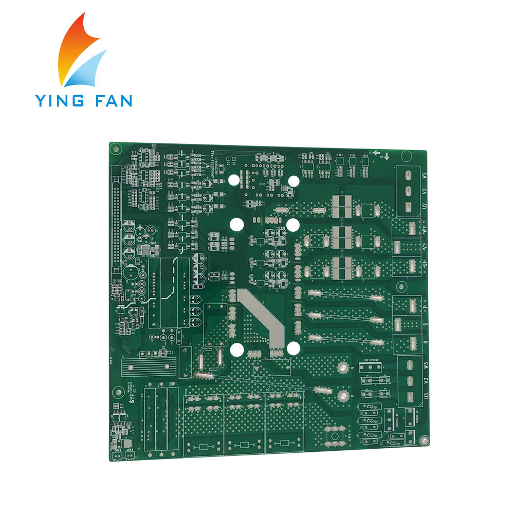
Thick copper PCB is single-sided, double-sided and multilayer printed circuit boards, flexible circuit boards, and buried blind via boards.
Process capability of thick copper PCB:
(1) Drilling: the minimum hole diameter of thick copper PCB is 0.15MM.
(2) Hole metallization: minimum hole diameter 0.15mm, plate thickness / hole diameter ratio 4: 1.
(3) Wire width: minimum wire width: gold plate 0.075mm, tin plate 0.10mm.
(4) Wire spacing: minimum spacing: gold plate 0.075mm, tin plate 0.10mm.
(5) Gold-plated plate: Nickel layer thickness: >or =2.5μ Gold layer thickness: 0.05-0.1μm or according to customer requirements.
(6) Spray tin plate: tin layer thickness:> or =2.5-5μ.
(7) Milling: Minimum distance from line to edge: 0.15mm Minimum distance from hole to edge: 0.2mm Minimum shape tolerance: ± 0.12mm.
(8) Socket chamfer: Angle: 30 degrees, 45 degrees, 60 degrees depth: 1 -3mm.
(9) V cut: angle: 30 degrees, 35 degrees, 45 degrees depth: plate thickness 2/3 minimum size: 80mm * 80mm.
(10) Solder resistance: 85---105℃ / 280℃---360℃.