HDI PCB is the English abbreviation of High Density Interconnector. High Density Interconnect (HDI) manufacturing is one of the fastest growing areas in the printed circuit board industry. HDI PCB is the English abbreviation of High Density Interconnector. High Density Interconnect (HDI) manufacturing is one of the fastest growing areas in the printed circuit board industry.
High-density interconnect (HDI) manufacturing in HDI PCB is one of the fastest growing areas in the printed circuit board industry. From the first 32-bit computer launched by Hewlett-Packard in 1985, to today's large client server with 36 sequential laminated multilayer printed boards and stacked micro-vias, HDI/micro-via technology is undoubtedly the future PCB architecture. Larger ASICs and FPGAs with smaller device pitches, more I/O pins and more embedded passive devices have shorter and shorter rise times and higher frequencies. They all require smaller PCB feature sizes, which promotes the Strong demand for HDI/micro vias.
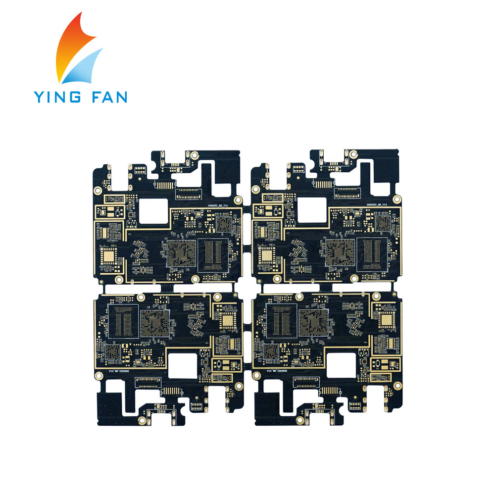
HDI process
First-order process: 1+N+1
Second-order process: 2+N+2
Third-order process: 3+N+3
Fourth-order process: 4+N+4